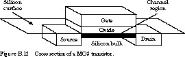
(a transistor gate bears no resemblance to a logic gate,
an unfortunately ambiguous use of the term).
The bottommost material layer is made of silicon, an insulating oxide layer
sits on top of it, and the topmost layer is the metal gate. (More
modern integrated circuit processes have replaced the metal layer with a
material called polycrystalline silicon, but the older "metal gate" terminology
still holds.) The source and drain regions contain silicon material
with a large excess of electrons separated by the slightly positively charged
bulk silicon. The source and drain are called diffusion regions because of the
chemical process used to create them. Negatively charged ions
(atoms with extra valence electrons) are placed onto
the silicon surface and are diffused into the surface by heating the silicon
material. The materials of the source and drain are identical. By convention,
the source is the electrical node with the lower of the two voltage potentials
at either end of the channel.
The electrical behavior of
the transistor is generally as follows. When a positive voltage is placed on the
gate, electrons from the silicon bulk are attracted to the transistor channel,
an initially nonconducting region between the source and drain very close to the
silicon surface. When the gate voltage becomes sufficiently positively charged,
enough electrons are pulled into the channel from the bulk to establish a
charged path between the source and the drain. Electrons flow across the
transistor channel, and the voltage-controlled switch is conducting. If a 0 or
very small voltage is placed on the gate, no electrons (or at least
very few) are attracted to the channel. The source and drain are
disconnected, no current flows across the channel, and the switch is not
conducting.
There are two fundamentally different kinds
of MOS transistors, called n-channel and p-channel transistors, or nMOS and pMOS
for short. Their schematic symbols are shown in Figure B.13.
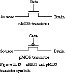
Because they are made from materials with different affinities for electrons,
the two transistor types behave quite differently. The transistor operation
described above is actually for the nMOS transistor. The bulk is positively
charged, while the diffusion is negatively charged. The transistor switch is
"closed" (conducting) when a logic 1 is placed on its
gate and "open" (nonconducting) when the gate is
connected to a logic 0. The pMOS transistor is complementary. The diffusion
regions are positively charged and the silicon bulk is negatively charged. A
pMOS transistor behaves in a complementary way: It is "closed"
(conducting) when a logic 0 is placed on the gate and
is "open" (nonconducting) when a logic 1 is placed
there.
The symbols for the two different kinds of
transistors make it easy to remember how they operate. An nMOS transistor
conducts when the gate voltage is asserted in positive logic. The pMOS
transistor conducts when the gate is asserted in negative logic. This is why
there is a polarity bubble on the gate of the pMOS transistor's
symbol.
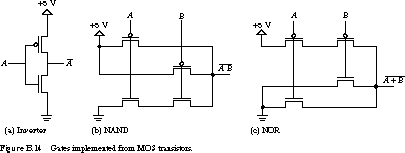
Figure B.14 shows transistor networks for (a) an
inverter, (b) a two-input NAND gate, and
(c) a two-input NOR gate. The power supply
(+5 V) and ground (0 V)
represent logic 1 and logic 0, respectively. The inverter is constructed from an
nMOS and a pMOS transistor connected in series between power and ground. It
operates as follows (see Figure B.15).
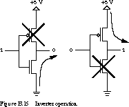
When A is a logic 1, the nMOS transistor is conducting and the pMOS
transistor is not. The only unbroken connection path is from ground to the
output node. Thus, a logic 1 at the input yields a logic 0 at the output.
Now let's look at the case in which A is a
logic 0. Now the pMOS transistor conducts while the nMOS transistor does not.
The output node is connected to a logic 1. A 0 at the input yielded a 1 at the
output. The series transistors implement an inverter.
The
transistor-level implementations of the NAND and NOR gate work similarly. Let's
start with the NAND logic gate, constructed from two nMOS transistors in series
between the output node and ground and two pMOS transistors in parallel between
the output node and the power supply. A path between the output node and ground
can be established only when both of the nMOS transistors are conducting. This
happens only if A and B are both at a logic 1. In this case,
the two pMOS transistors are not conducting, breaking all paths between the
output node and the logic 1 at the power supply. This is the case A
= B = 1, output = 0.
Now what happens if one or both of A and B are at
a logic 0? Let's take the case A = 0 and B
= 1 (see Figure B.16).
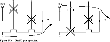
The nMOS transistor controlled by A is not conducting, breaking the
path from the output to ground. The pMOS transistor it controls is conducting,
establishing the path from the power supply to the output. The other path,
controlled by B, is broken, but this has no effect on the output node
as long as some path exists between it and some voltage source.
The case A = 1 and B =
0 is symmetric. If both inputs are 0, there are now two paths between the power
supply's logic 1 and the output node. Of course, this doesn't change the logic
signal at the output: it is still a logic 1. From this discussion it should be
obvious that the circuit configuration performs the function of a NAND
gate.
The pull-down network switches between the output
and the ground signal. We define the pull-up network similarly between the
output and the power supply. The pull-down network is A B,
since the transistors are two nMOS transistors in series. The pull-up network
consists of two pMOS devices in parallel. This logic function is ![]() . Another way to say this is that the function is 0
when A B is true and is 1 when
. Another way to say this is that the function is 0
when A B is true and is 1 when ![]() is true. Of course, by DeMorgan's theorem,
is true. Of course, by DeMorgan's theorem, ![]() is the same function as
is the same function as ![]() .
.
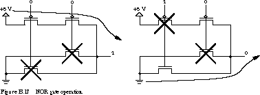
We can apply the same kind of
analysis to the NOR gate implemented as transistors. Using the observation we
just made, the pull-up network is ![]() , the pull-down network is A
, the pull-down network is A +
B, and the function is 0 when A + B is
true and is 1 when ![]()
(![]()
) is true. Analyzing the transistor network
directly (see Figure B.17), the output node can be 1
only if both transistors between it and the power supply are conducting. Thus
the output is 1 if both inputs are 0. If either or both inputs are 1, then the
path to the power supply is broken while at least one path from the output to
ground is established. The network does indeed implement the NOR function.
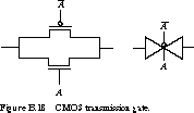
The pMOS and nMOS transistors are connected in parallel and are controlled by
complementary control signals in the figure. When signal A is asserted,
the transmission gate conducts a logic 0 or 1 equally well. Signal A at
a logic 1 makes the nMOS transistor conduct, while ![]() at a logic 0 makes the parallel pMOS transistor conduct as well. When A
is unasserted, the gate no longer conducts. A at logic 0 breaks the
connection through the nMOS transistor, while
at a logic 0 makes the parallel pMOS transistor conduct as well. When A
is unasserted, the gate no longer conducts. A at logic 0 breaks the
connection through the nMOS transistor, while ![]() at 1 has the same effect on the pMOS transistor. In circuit diagrams, the
transmission gate is often denoted by a "butterfly" or "bow tie" symbol, as
shown in the figure.
at 1 has the same effect on the pMOS transistor. In circuit diagrams, the
transmission gate is often denoted by a "butterfly" or "bow tie" symbol, as
shown in the figure.
Section 4.2 covers how to use CMOS
transmission gates to implement digital subsystems with many fewer transistors
than would be the case if traditional gates were used.
[Top]
[Next]
[Prev]