(current) flows through the spigot. The transistor is
in its "off" region of operation. As the screw is turned, the flow of water
begins to trickle and then increases. This is the so-called linear operating
region. The current increases linearly as the voltage across the transistor is
increased. Eventually, the flow reaches a point where opening the screw further
does not increase the flow, it being limited by the diameter of the pipe. This
is called the saturation region. Despite changes in voltage across the
transistors, there is no change in current. Transistors in digital logic pass
quickly from the off region to the saturation region.
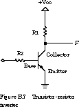
The basic inverter constructed from transistors and resistors
is shown in Figure B.7 (for those in the know, the transistor shown
is an NPN transistor).

A high voltage at the base turns on the transistor. The output F is
discharged to ground, getting close to 0 V but never quite reaching it
(it reaches a voltage drop away from 0 V).
When a low voltage is placed on the base, the transistor is
turned off. The output node F is charged up toward the power supply
voltage through the pull-up/load resistor R1.
(not AND) and NOR (not
OR) functions.
A two-input DTL (diode-transistor
logic) NAND gate is shown in Figure B.8.
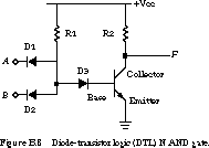
It works like this. The diodes marked D1 and D2, together with resistor R1, form a two-input AND function. At the input to D3, a logic 0 is represented by approximately 0.7 V, while a logic 1 is in the range 4 to 5 V. D3 increases the voltage required to turn on the transistor. This gives a better separation between the voltage levels recognized as a logic 0 and logic 1.
For the transistor to conduct, D3 must be turned on. This
happens when the anode voltage reaches 1.4 V. If the voltage at the anode is
much higher than this, the base will be driven to a high voltage. The transistor
will be strongly turned on, with low resistance, and thus F will be
discharged toward 0 V. If the anode is at a low voltage, the base will also be
low. This keeps the transistor off (essentially infinite
resistance), allowing the output node to reach a logic 1 voltage
level.
Gates constructed as in Figure B.8 have a limit to
the number of gate inputs to which their output can be connected. This is called
fan-out. The pull-up resistor R2 is what limits the fan-out. The output
F is at Vcc as long as no current is being drawn from the power supply
to charge electrical nodes to which F is connected. However, if
F is connected to the A or B input of a similar gate,
current is drawn through R2. The voltage at F is reduced according to
Ohm's law. If there are too many connections drawing current, the voltage at
F may be so reduced that it can no longer be recognized as a logic 1.
Thus, the number of fan-outs must be carefully limited in this kind of
logic.
DTL has several advantages. NAND and NOR
functions, which are easy to build in DTL, are logically complete. This means
that any logical function can be expressed as a collection of only NAND gates or
only NOR gates. NAND and NOR gates form the heart of all logic designs. In
addition, this logic family uses lower voltages, less power, and operates at
higher speeds, since only small currents are needed to turn on the transistors.
Another feature of DTL is its ability to implement a "wired AND" function. For example, if we wired several DTL NAND gates together, we would observe the following behavior. If any one of the NAND gates had a logic 0 as its output, the whole output function would also be at a logic 0 voltage. All the output functions would have to be at logic 1 for the output to be 1. See Figure B.9, which shows the internal wiring and the equivalent logic schematic for the wired AND function.
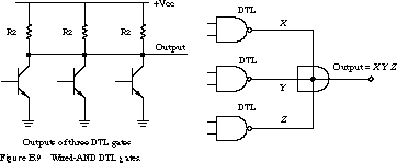
The AND gate does not actually exist. The notation is used simply to represent that the interconnection forms the AND function.
(TTL), and it is the most widely used family of
components available today.
A two-input TTL NAND gate is shown in Figure B.10
(some of the details have been eliminated).
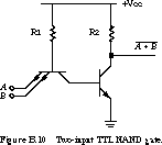
This circuit replaces the three diodes of Figure B.8 with a dual emitter transistor. This configuration has one significant advantage over the diode implementation. Besides being voltage--controlled switches, transistors also act as amplifiers. When the transistor base is undergoing a change in voltage, the transistor can amplify this change, thus speeding up the rate at which the transistor turns on or off. The result is faster gate switching.
In simplified terms, the circuit of Figure B.10 works as follows. When one of the inputs A or B is low, the current available through R1 at the transistor base is diverted to ground. No current flows from the base to the collector, and therefore no current reaches the base of the output transistor. Thus, the output transistor is off. The pull-up resistor R2 charges the output node to the high-voltage state. Only when both inputs are high can the current flow through R1 from base to collector to turn on the output transistor. In this case, the output path discharges to ground.
A more realistic circuit for a NAND logic gate, such as that found in the TTL 7400 component, is shown in Figure B.11.
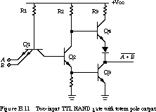
The output configuration with transistor Q4 in the pull-up path and transistor Q3 in the pull-down path is called a totem pole output. Q4 makes it possible to pull up the output faster, using lower power than is possible with just a resistor. In principle, this circuit behaves much like the simplified schematic of Figure B.10.
In Section 4.2.4, we introduce the concept of open-collector
gates. These are gates with internal organizations that allow them to
participate in a wired-AND configuration, similar to the DTL gates in Figure
B.9. The pull-up path, namely the R3 resistor, Q4 transistor, and the diode of
the output stage of Figure B.11, is eliminated in an open-collector gate. Thus,
an open-collector gate only has the ability to pull down its output node. We
need a resistor external to the gate. This pulls up the wired-AND output if none
of the attached gates have an input combination that provides a pull-down path
to ground.
Section 4.2.4 also introduces the concept of
tri-state gates. These are gates with three possible interpretations of their
outputs: logic 0, logic 1, and no connection. The latter is called the
high-impedance state and is -denoted by the "value" Z. In Figure B.11,
the totem pole output transistors Q3 and Q4 are not designed to be on
simultaneously. Q4 is on when the output is 1, and Q3 is on when the output is
0. In a tri-state gate, both of these transistors can be off at the same time
when a special enable input is left unasserted. The output node is disconnected
from +Vcc or ground, making it appear to other logic as an open
circuit.
(0-70\xa1 C), voltage
range (5 V ± 5%), loading, and the parametric variance
of the semiconductor devices themselves.(output high
voltage) is the minimum voltage at which the circuit delivers a
logic 1. Vol (output low voltage) is the
maximum voltage at which the circuit can produce a logic 0.(input high
voltage) is the minimum voltage at which a circuit detects a logic
1. Vil (input low voltage) is the maximum
voltage at which it recognizes a logic 0.= 2.4 V, Vol = 0.4 V,
Vih = 2 V, and Vil = 0.8 V. The
input and output voltages differ by 0.4 V. This permits the output signals to be
degraded by the wires between circuits but still be recognized as good logic
values. The difference between Voh and Vih is called the
high-state DC noise margin. The difference between Vol and Voh
is called the low-state DC noise margin.